- 您现在的位置:买卖IC网 > Sheet目录1991 > CS4362A-DQZ (Cirrus Logic Inc)IC DAC 6CH 114DB 192KHZ 48-LQFP
6
ICS97U870
Advance Information
0817—07/07/03
Notes:
1.
Switching characteristics guaranteed for application frequency range.
2.
Static phase offset shifted by design.
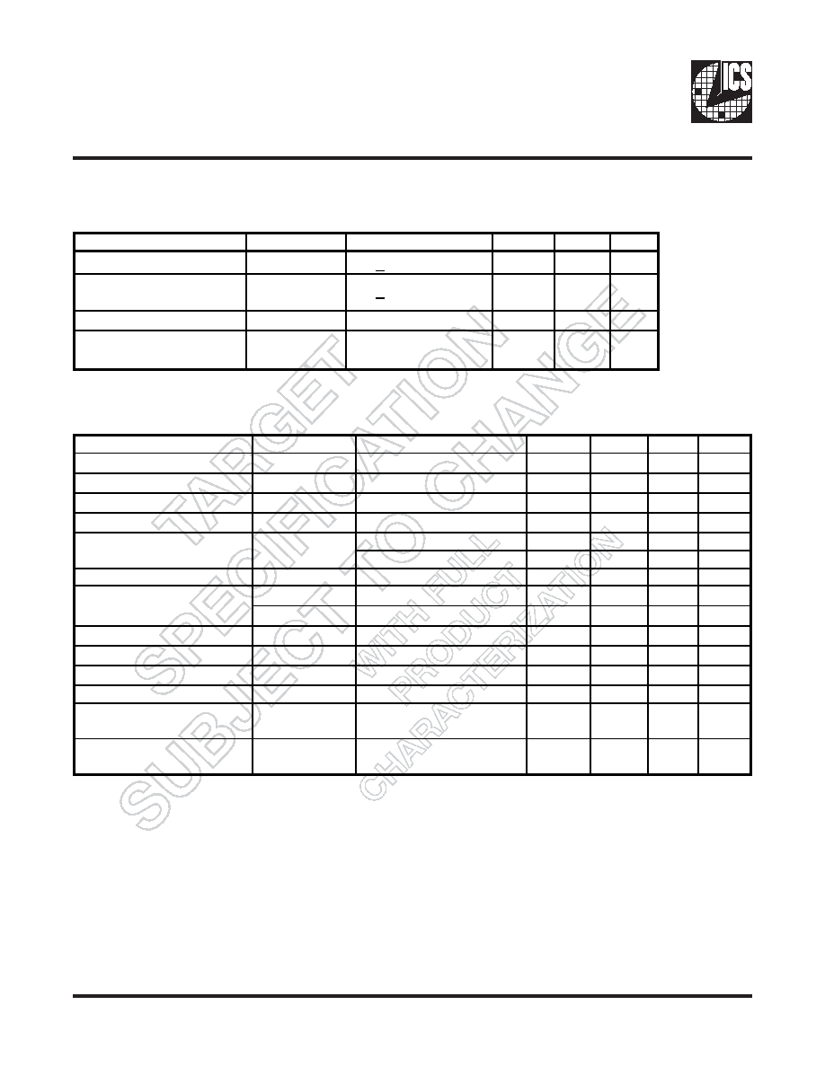
Timing Requirements
TA = 0 - 70°C Supply Voltage AVDD, VDDQ = 1.8 V +/- 0.1V (unless otherwise stated)
PARAMETER
SYMBOL
CONDITIONS
MIN
MAX
UNITS
Max clock frequency
freqop
1.8V+0.1V @ 25°C
95
370
MHz
Application Frequency
Range
freqApp
1.8V+0.1V @ 25°C
160
350
MHz
Input clock duty cycle
dtin
40
60
%
CLK stabilization
TSTAB
15
s
Switching Characteristics
1
TA = 0 - 70°C Supply Voltage AVDD, VDDQ = 1.8 V +/- 0.1V (unless otherwise stated)
PARAMETER
SYMBOL
CONDITION
MIN
TYP
MAX
UNITS
Output enable time
ten
OE to any output
4.73
8
ns
Output disable time
tdis
OE to any output
5.82
8
ns
Period jitter
tjit (per)
-30
30
ps
Half-period jitter
tjit(hper)
-60
60
ps
Input Clock
1
2.5
4
v/ns
Output Enable (OE), (OS)
0.5
v/ns
Output clock slew rate
SLr1(o)
1.5
2.5
3
v/ns
tjit(cc+)
040
ps
tjit(cc-)
0
-40
ps
Dynamic Phase Offset
t( )dyn
-20
20
ps
Static Phase Offset
tSPO
2
-50
0
50
ps
Output to Output Skew
tskew
40
ps
SSC modulation frequency
30.00
33
kHz
SSC clock input frequency
deviation
0.00
-0.50
%
PLL Loop bandwidth (-3 dB
from unity gain)
2.0
MHz
Cycle-to-cycle period jitter
Input slew rate
SLr1(i)
发布紧急采购,3分钟左右您将得到回复。
相关PDF资料
CS4364-CQZR
IC DAC 103DB 24BIT 6CH 48-LQFP
CS4382A-DQZ
IC DAC 8CH 114DB 192KHZ 48-LQFP
CS4384-CQZR
IC DAC 8CH 103DB 192KHZ 48-LQFP
CS4385-DQZR
IC DAC 8CH 114DB 192KHZ 48-LQFP
CS4391A-KZZR
IC DAC 24BIT 192KHZ W/VC 20TSSOP
CS4392-KZZ
IC DAC 24BIT 192KHZ W/VC 20TSSOP
CS4397-KSZ
IC DAC 24BIT MULTY STNDRD 28SOIC
CS4398-CZZ
IC DAC 120DB 192KHZ W/VC 28TSSOP
相关代理商/技术参数
CS4362A-DQZR
功能描述:数模转换器- DAC IC 114dB 192 kHz 6Chn DAC w/DSD supt RoHS:否 制造商:Texas Instruments 转换器数量:1 DAC 输出端数量:1 转换速率:2 MSPs 分辨率:16 bit 接口类型:QSPI, SPI, Serial (3-Wire, Microwire) 稳定时间:1 us 最大工作温度:+ 85 C 安装风格:SMD/SMT 封装 / 箱体:SOIC-14 封装:Tube
CS4362A-EQZ
制造商:CIRRUS 制造商全称:Cirrus Logic 功能描述:114 dB, 192 kHz 6-channel D/A Converter
CS4362A-EQZR
制造商:CIRRUS 制造商全称:Cirrus Logic 功能描述:114 dB, 192 kHz 6-channel D/A Converter
CS4362-BQ
制造商:CIRRUS 制造商全称:Cirrus Logic 功能描述:114 dB, 192 kHz 6-Channel D/A Converter
CS4362-KQ
制造商:Cirrus Logic 功能描述:114 DB, 24-BIT, 192 KHZ, 6- & 8-CHANNEL D/A CONVERTER - Rail/Tube
CS4362-KQZ
功能描述:数模转换器- DAC IC 114dB 192kHz 6Ch DAC RoHS:否 制造商:Texas Instruments 转换器数量:1 DAC 输出端数量:1 转换速率:2 MSPs 分辨率:16 bit 接口类型:QSPI, SPI, Serial (3-Wire, Microwire) 稳定时间:1 us 最大工作温度:+ 85 C 安装风格:SMD/SMT 封装 / 箱体:SOIC-14 封装:Tube
CS4362-KQZR
功能描述:数模转换器- DAC IC 114dB 192kHz 6Ch DAC RoHS:否 制造商:Texas Instruments 转换器数量:1 DAC 输出端数量:1 转换速率:2 MSPs 分辨率:16 bit 接口类型:QSPI, SPI, Serial (3-Wire, Microwire) 稳定时间:1 us 最大工作温度:+ 85 C 安装风格:SMD/SMT 封装 / 箱体:SOIC-14 封装:Tube
CS4364
制造商:CIRRUS 制造商全称:Cirrus Logic 功能描述:103 dB, 192 kHz 6-Channel D/A Converter